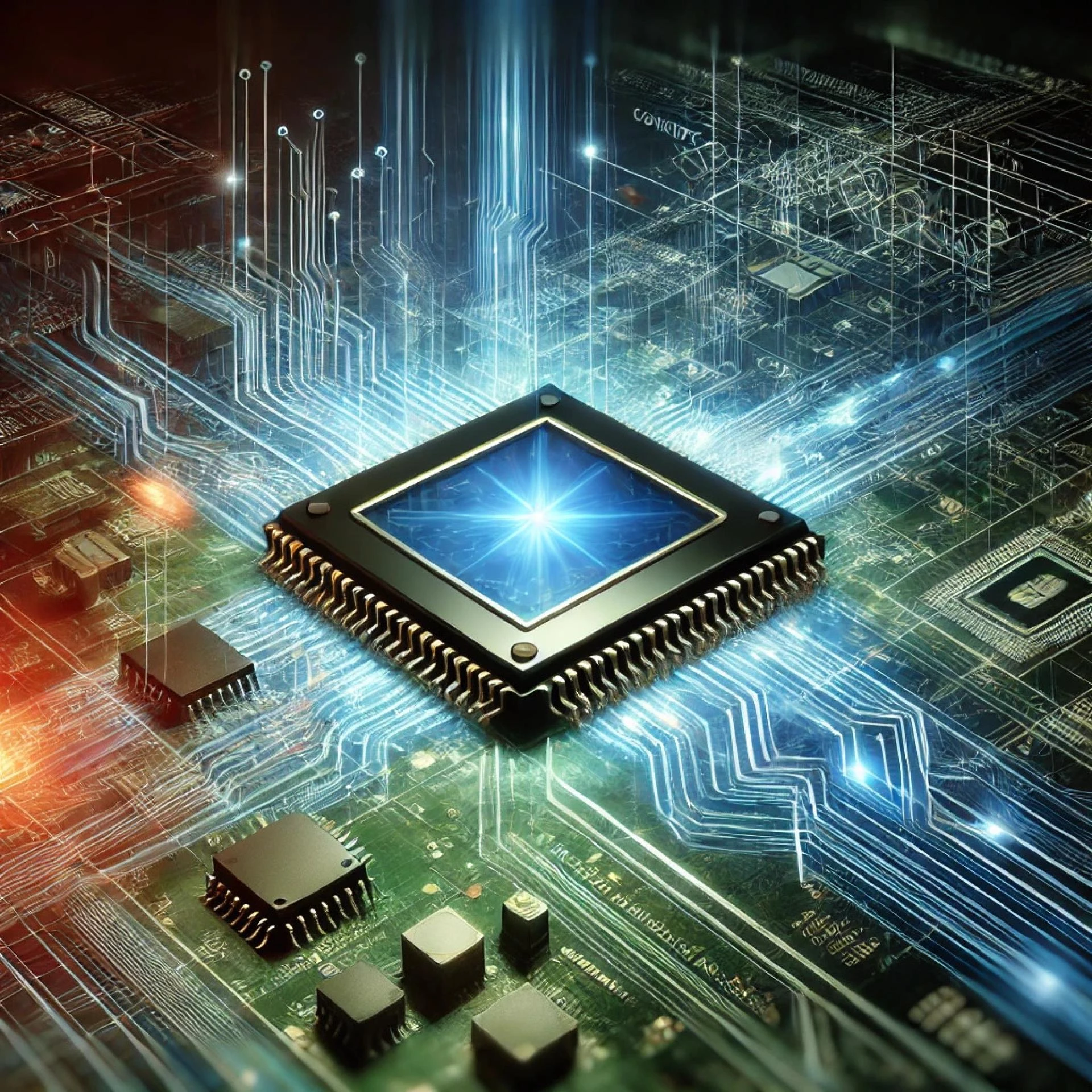
 Bringing Ideas to Life with FPGA Design & Development
Imagine turning your vision into a working digital system—without waiting years for custom silicon. That’s the power of FPGA Design & Development. Field Programmable Gate Arrays (FPGAs) bridge the gap between software and hardware, offering flexibility, speed, and customization. But how does an idea evolve from concept to silicon? Let’s break it down.
1. Defining the Concept
Every design begins with an idea. Whether it's a high-speed data processor, a machine learning accelerator, or a real-time signal processor, the first step is defining FPGA Design & Development goals. Questions like:
- What problem does the FPGA need to solve?
- What are the performance and power constraints?
- Which FPGA family best fits the requirements?
Once the concept is clear, the design process moves forward.
2. Choosing the Right FPGA
Not all FPGAs are created equal. Selecting the right one depends on factors like logic capacity, processing power, and power efficiency. Designers evaluate available FPGA options, considering whether they need high-performance DSP blocks, embedded memory, or specific I/O interfaces.
3. Architecture and Design Entry
Now, the real work begins. Engineers define the architecture, mapping out how different components will interact. This stage involves:
- Designing using FPGA Design & Development tools like HDL (Hardware Description Language)
- Creating block diagrams for logic implementation
- Planning data paths and optimizing for speed and efficiency
4. Simulation & Verification
Before moving to physical implementation, every FPGA design undergoes rigorous simulation and verification. Engineers test logic functionality, timing, and performance using simulation tools. This helps catch errors early, saving valuable time.
5. Synthesis & Implementation
Once the design is verified, it is synthesized—converted from HDL into a netlist that can be mapped onto FPGA hardware. The next steps include:
- Placement & Routing: Mapping logic gates to FPGA resources
- Timing Analysis: Ensuring the design meets speed constraints
- Power Optimization: Reducing unnecessary power consumption
6. FPGA Bitstream Generation
With the implementation finalized, the design is transformed into a bitstream—a file that programs the FPGA. This step essentially “burns” the logic into the programmable fabric, bringing the design to life.
7. Hardware Testing & Debugging
Now, the moment of truth. The programmed FPGA is tested on hardware, ensuring real-world functionality. Debugging tools like logic analyzers and on-chip debugging features help refine the design. If issues arise, designers iterate, making adjustments and reprogramming the FPGA.
8. Optimization & Deployment
Once testing is complete, the design undergoes final optimizations for performance, efficiency, and reliability. Whether the FPGA is part of an embedded system, a high-performance computing setup, or an industrial application, this stage ensures smooth deployment.
Wrapping Up
From concept to silicon, FPGA Design & Development transforms ideas into functional hardware solutions. Whether for prototyping, acceleration, or specialized computing, FPGAs play a crucial role in modern electronics. With the right approach, expertise, and tools, the journey of custom FPGA design becomes an exciting and rewarding process.
Need an FPGA solution? Start designing today!
FAQs About Custom FPGA Design
1. How long does the FPGA Design & Development process take?
Timelines vary depending on design complexity. Some projects take weeks, while others require months of development and testing.
2. What are the benefits of using FPGAs over traditional ASICs?
FPGAs offer flexibility, faster time-to-market, and reprogrammability—unlike ASICs, which require fixed silicon and long fabrication cycles.
3. Can FPGAs be reprogrammed after deployment?
Yes! That’s one of their biggest advantages. Updates and modifications can be made post-deployment, making them ideal for evolving applications.


Sign in to leave a comment.