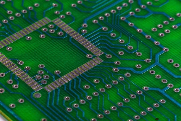
Printed Circuit Boards (PCBs) are the life line of today’s electronics, actually a base /substrate on which the electronic components are mounted and interconnected as per desired functional requirement. Since the electronic products are getting more sophisticated and miniaturized, so the concept of PCB must change to improve the performance and reliability. Another important issue concerning the development of the most recent levels of PCB manufacturing is via fill and via plug. They are crucial for optimising and enhancing the electrical characteristics, mechanical characteristics and reliability of PCBs particularly in HD and HS technologies. In this system level approach, we will begin with the definition of the via filling and via plugging process along with the advantages of the systems, the types of systems used and its application in the advanced industries.
Introduction to Vias in PCBs
Definitions and Types of Vias
Vias are the small blind holes that are drilled in to the PCBs with the purpose of providing connection path between the layers within the board. They are needed in the complex design of today’s PCBs and relay signals and power through the board. The main types of vias include:
Through-Hole Vias: These go from the upper plane to the lower one of the PCB.Blind Vias: These pass from one side of the board to another but do not pass through the layers in between.Buried Vias: These link the inner layers, but do not cover the outer layers.Microvias: Also called micro-vias, they are smaller than a standard via and are employed in HDI PCBs.Importance of Vias in PCB Design
PCB Via Filling are also critical when it comes to multi-layer PCBs as they provide the necessities for their functioning. It is used to provide pathways for transmitting electrical signals and power between layers and helps to define the most efficient connections and avoid signal crossover. It indicates that as the complexity level of PCBs increases, the function of vias is more significant in the functionality and durability of the electronics components.
What is Via Filling and Via Plugging?
Definition and Differences
Via Filling
The procedure of sealing holes with a filler material that can either be a conductor or an insulator to increase the circuit board’s electronic and mechanical characteristics. Conductive filling is common for better signal integrity and thermal conduction while non-conductive filling offers support to the structure and also avoid contamination.
Via Plugging
The action of filling via with some material to close it to avoid solder carry during assembly or to level up the PCB board. Plugging materials can also be either conducting or non-conducting types.
Why They Are Necessary
Via filling and plugging are necessary for several reasons:
Improved Electrical Performance: Conductive via filling truly helps the signal integrity while reduces the resistance.Mechanical Strength: As for some forms of vias, they are filled to ensure rigidity or make them stronger.Prevention of Solder Wicking: Plugged vias do not allow solder to flow through via during assembly, and hence offering a strong solder joint.Enhanced Reliability: Each process is useful in complementing the other in the enhancement of the durability and dependability of the PCB especially where the application is subject to extreme conditions.Benefits of Via Filling and Via Plugging
The following are the Pros of Via Filling and Via Plugging
Electrical Performance
With the help of filling, especially with conductive materials, as stated previously, the electrical characteristics of PCBs are enhanced. It minimizes the resistance as well as inductance of via but the matter is significant in the high frequency applications. It also improves thermal conductivity of vias aiding in dissipation of heat and also reduces voids in the conductive filling improving the via filling.
Mechanical Strength
Thus, filling and plugging of through-hole reduces the mechanical stress on PCB, otherwise, crack like mechanical failure is quite possible. This is especially relevant in situations where PCBs ought to be installed in harsh conditions or wherever physical shock may be expected.
Reliability and Durability
Via filling and plugging provide great benefits in the reliability and durability or PCBs. These processes give the vias shield from the external environment, which in one way or another may pose a threat to the performance of the circuits, such as humidity. This is particularly important for applications where safety is paramount as in Aerospace, Automobile and Medical equipment.
Applications of Via Filling and Via Plugging
These are the applications of Via Filling and Via Plugging
High-Density Interconnect (HDI) PCBs
A PCB developed through HDI PCB technique incorporates more layers with denser lines and spaces so that more numbers of components can be incorporated within a small area. More specifically, filling and plugging are crucial in the process of the formation of HDI technology in order to guarantee the good electrical contacts and avoid defects.
High-Frequency and High-Speed PCBs
In high-frequency and high-speed applications, signal integrity is paramount. Conductive via filling helps maintain the quality of high-speed signals by reducing resistance and inductance.
Rugged and High-Reliability Applications
PCBs used in applications like aerospace and military are exposed to harsh situations; therefore, mechanical strength and reliability are important aspects. Access, through the method of filling and plugging ensures therightness of these PCBs by offering needed reinforcement as well as safety to guarantee that they offer what has been contracted even under some of the worst conditions.
Methods of Via Filling
These are the methods of Via Filling
Conductive Via Filling
Conductive via filling itself means to fill the via with a conductive medium like Copper paste. This method is used in order to enhance electrical connections and thermal performance of the device as well. Conductive via filling is used mainly in high performance applications, where signal path and thermal conductivity are very important.
Non-Conductive Via Filling
Non-conductive via filling employs epoxies to fill the vias. As to its advantages, this method offers the reinforcement of the structure and protection against contamination while its disadvantage is that electrical conductivity is not boosted. It is mostly utilised in cases where issues such as mechanical strength and dependability are most vital.
Semi-Additive and Additive Methods
Semi-additive and additive are some of the more complex techniques utilized in via filling. These methods include the techniques of technology build up and deposition technique where thin layers of material are deposited systematically to form vias. site They provides accurate control of the filling process and are applicable to high density and high precision PCBs.
Methods of Via Plugging
These are the methods of Via Plugging
Solder Mask Plugging
Solder mask plugging entails blocking of the vias by using solder mask material. This method is widely utilized to avoid situations when the solder penetrates into the via, which is specifically applied in making micro-vias, as well as to enhance the flatness of the multilayer PCB. For most general uses, solder mask plugging is an inexpensive method of meeting the needs of many PCB designs.
Resin Plugging
In resin plugging, epoxy resin is applied to paste and Block the vias. This method is characterised by good mechanical strength and reliability, and thus suitable for applications which require high reliability. It is also a good baits in thermal and electrical insulation respectively.
Conductive Paste Plugging
If through holes are electrically connected through each of the layers, then conductive paste plugging could be used where a paste such as a silver or copper paste fills the through hole. This procedure is a combination of conductive via filling and the efficiency of via plugging in sealing the board. Thus, it is suitable for applications with high electrical performance and reliability.
Materials Used in Via Filling and Plugging
Types of Fillers and Plugs
Various materials are used for via filling and plugging, including:
Copper Paste: Applied for the conductive via filling to improve the electrical and thermal conductivity.Epoxy Resin: Employed for non-conductive via filling and usage of resin for via plugging since they offer mechanical strength and electrical insulation.Solder Mask: They are used in solder mask plugging to avoid solder wicking and in addition enhance the smoothness of the surface.Conductive Paste: Used for the conductive paste plugging that integrates the electrical characteristic with the mechanical gear allowing.Selection Criteria
The choice of material for via filling and plugging depends on several factors, including:
Electrical Requirements: Special emphasis is placed on the conductive material for applications where better electrical conductivity is desired.Mechanical Strength: High mechanical strength is offered by material selected in exterior or general purpose, high reliability required applications.Thermal Management: Thermal conductivity of the material is important criterion which is considered to select the material for the application where heat dissipation is required in larger amount.Cost and Availability: This includes the issue of cost in relation to the type of material required and the availability of the same as another limitation.Process Steps for Via Filling and Plugging
These are the process steps for Via Filling and Plugging
Preparation
The preparation stage entails washing the PCB to enable it get rid of dust or any other debris that may have accumulated on it and cleaning of the via to enable it open. The second step must be carried accurately to ensure the correct interconnect and filled vias.
Filling and Plugging
Filling and plugging entails applying the selected material to the via’s, and it could be through screen printing or stencil printing or even by injection. Once the material has been delivered to the vias it is left to settle and compact so as to offer a complete filling of the vias.
Curing and Inspection
Following on the filling and plugging process, the PCB is exposed to a high temperature to set the material. This can be through thermal curing, ultraviolet curing and may other ways depending on the material used. After the exposure and development steps are complete, the PCB is inspected for proper filling and plugging of the vias and for defects.
Challenges and Solutions in Via Filling and Plugging
Common Issues
Some common challenges in via filling and plugging include:
Void Formation: This results in formation of voids and such are undesirable as they affect the electrical and mechanical performance of the vias.Material Shrinkage: Due to shrinkage some materials contract at curing zone, hence may not fill the desired volumes or crack.Adhesion Issues: If the filling/plugging material does not stick well to the via walls, delamination or voids will occur.Thermal Mismatch: Thermal expansion discrepancies between the PCB substrate is and the filling/plugging materials can accommodate stress and possible failures under thermal stress.Best Practices
To address these challenges, manufacturers can adopt the following best practices:
Proper Cleaning and Preparation: It is important to avoid shorts, bad contacts, and voiding, and to avoid interfacing materials that will not adhere during the filling process by cleaning the via.Material Selection: Selecting materials for the composite having similar thermal expansion coefficients and low shrinkage can also minimize the thermal mismatch and voids.Controlled Application: Hence to reduce the magnitude of voids in the filled structures, proper application methods and equipment should be employed to produce controlled fills.Thorough Curing: In this step, proper curing processes and the correct curing times to allow the materials to harden and bond to the via walls.Regular Inspection:Ensuring that firms establish strict checks and inspections such as the use of X-ray and thermal imaging to identify the problems early in the production line.Future Trends in Via Filling and Plugging Technology
Innovations and Emerging Techniques
The field of via filling and plugging is fairly recent with newer versions of the method as well as newer techniques being developed to enhance on the earlier methods. Some emerging trends include:
Advanced Conductive Materials: Controlling the property of electrical and thermal conductivity to enhance the new conductive pastes and fillers.Automated Processes: The very obvious improvement with the increase in automation was that the precision, consistency and the rate at which the via was filled and plugged was enhanced.Nanotechnology: Application of nanomaterials to improve the possibility of filling structure and the properties of the materials.Eco-friendly Materials: Studies on the use of environmentally friendly materials for filling and plugging so as to minimize on the effects that PCB manufacturing has on the environment.Impact on PCB Manufacturing
These are premised to offer a boost in the manufacturing of PCBs due to the enhanced reliability and superior performance. Advanced materials and technologies will enable further scaling, higher signal quality, and better heat dissipation to satisfy the requirements of advanced electronic products.
Conclusion
Filling and plugging are the significant steps in the highly developed method of PCB production and help in improving electrical characteristics, mechanical properties, and durability. Thus, as electronics continues to advance, the use of these techniques will only increase, which will guide additional advancements in PCB technology. Thus, by getting familiar with the elements, which form the basis of via filling and plugging, one can enhance his/her manufacturing processes and develop PCBs that conform to the requirements of the contemporary market.
Here are detailed definitions and benefits of via filling and plugging, as well as the methods of implementing this approach, and a prediction of the tendencies that future industrial processes have in store for manufacturing top-notch PCBs.


Sign in to leave a comment.